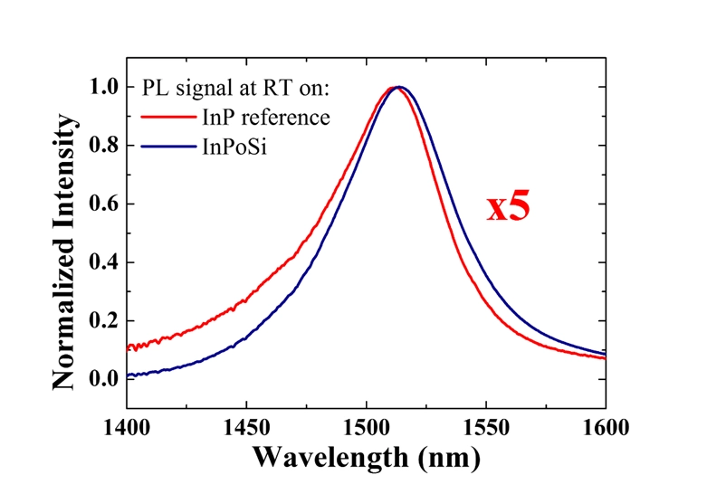
DFB RIDGE LASER DIODES AT 852 NM AND 894 NM FOR CESIUM ATOMIC CLOCKS
We have demonstrated DFB Ridge laser diodes emitting at 852nm and 894nm, at room temperature, and their packaging in hermetic TO-3 can, addressing the pumping of Cs. These lasers respond to all specifications required for the realization of very stable optically pumped compact industrial Cesium beam atomic clocks. Indeed, they show a low threshold current, a high external differential efficiency,
with emission in a single spatial mode and in a single frequency, with a very high side mode suppression ratio and a linewidth less than 1MHz.
REFERENCE: M. Garcia, C. Theveneau, P.A. Roxo, A. Larrue, P. Resneau, Y. Robert, E. Vinet, J.P. Legoec, O.Parillaud, B. Gérard, M. Krakowski
"DFB RIDGE LASER DIODES AT 852 NM AND 894 NM FOR CESIUM ATOMIC
CLOCKS"
OPTRO2020 paper 45
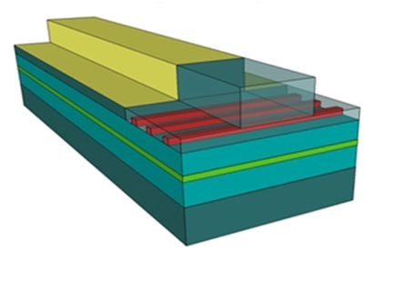
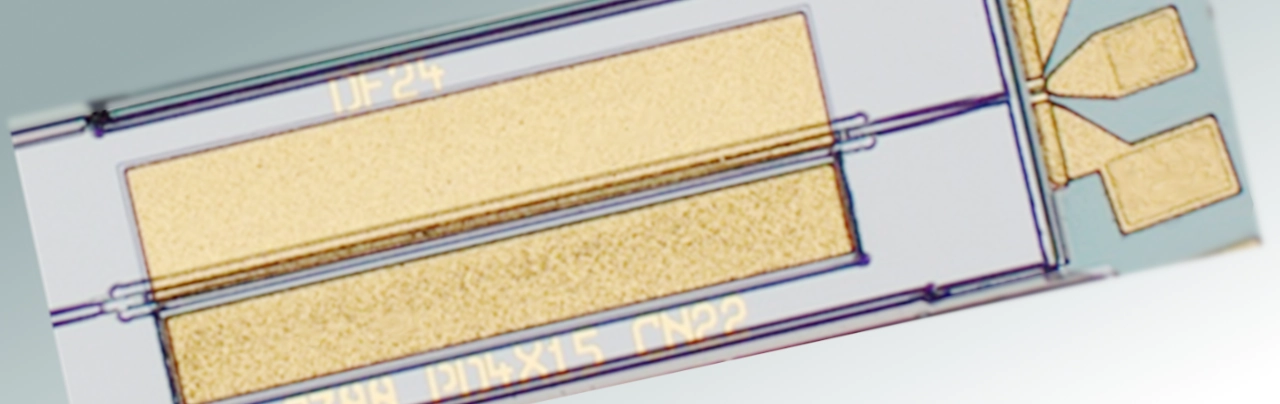
Schematic view of the ridge DFB laser with Aluminium free active region
(Quantum Well: GaInAsP, Optical Confinement: GaInP) grown by two steps Metal Organic Vapor Phase Epitaxy (MOVPE)
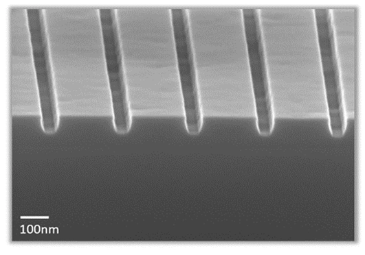
Scanning Electron Microscopy (SEM) picture of the Bragg grating realized by e beam lithography
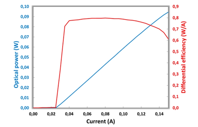
Light- current and efficiency-current characteristics showing low threshold current and high efficiency of the DFB laser emitting at 852nm
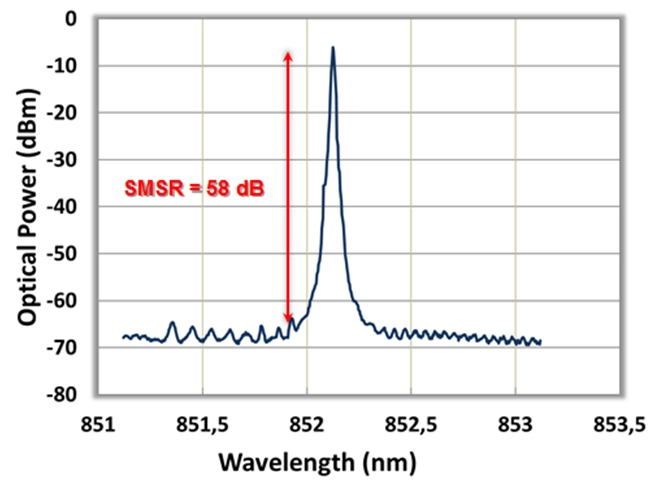
Optical spectrum at 22°C and 75mA showing an emission at 852.12nm (Cs D2 line) with a very high rejection of the side modes
Record Pulse Energy (201pJ) Passively Mode-Locked Monolithic Tapered Laser
We demonstrate a very-long (13.5 mm) monolithic multi-section tapered laser reaching 201pJ mode-locked (ML) pulses at low repetition frequency of 2.89 GHz with a pulse width of 11ps (compressed to 2.4ps). To the best of our knowledge, this is the first demonstration of a fundamental frequency ML at such low PRF in a centimeter-long monolithic semiconductor laser. This is also a demonstration of a record high pulse energy from the electrically pumped laser diode without any additional amplification stage.
REFERENCE: Michel Krakowski , Patrick Resneau, Michel Garcia, Eric Vinet, Yannick Robert, Olivier Parillaud, Bruno Gérard, Stefan Kundermann, Nicolas Torcheboeuf , and Dmitri L. Boiko
"Stabilized High Pulse Energy Passively Mode-Locked Monolithic and External Cavity Tapered Lasers for Space Applications"
IEEE JOURNAL OF SELECTED TOPICS IN QUANTUM ELECTRONICS, VOL. 25, NO. 6, NOVEMBER/DECEMBER 2019
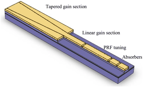
Schematic diagram of the very long (13.5mm) monolithic multi-sections tapered laser
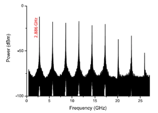
RF spectrum of the monolithic multi-section tapered laser. Pulse Repetition Frequency is 2.886GHz thanks to the very long laser cavity.