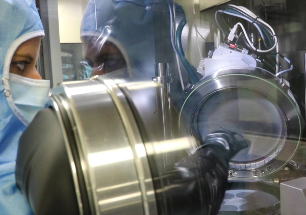
Epitaxy
Unique expertise of III-V material growth covering a wide variety of semiconductor compounds based on:
- InP Indium Phosphide,
- GaAs Gallium Arsenide,
- GaN Galium Nitride...
This growth is realised on III-V substrates as well as on advanced substrates (thin InP films bonded on Si or SOI).
Wide range of epitaxy reactors (x8) MBE (Molecular Beam Epitaxy), MOVPE (Metalorganic Vapor Phase Epitaxy), GSMBE (Gas Source Molecular Beam Epitaxy) reactors for state of the art III-V material research activities.
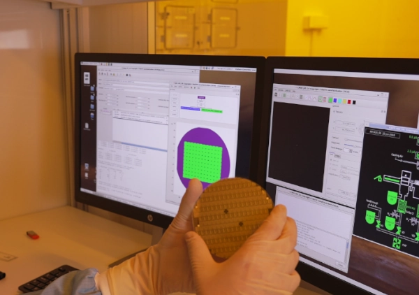
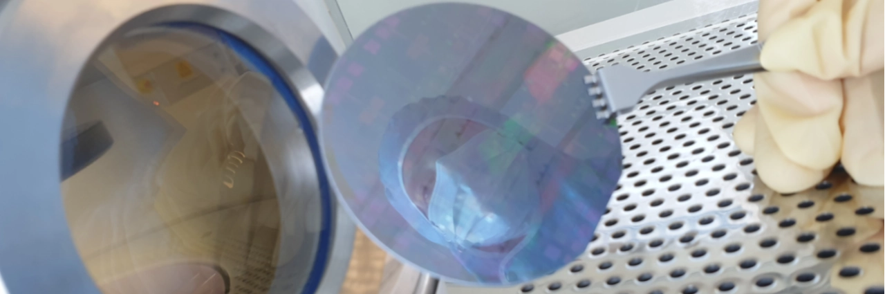
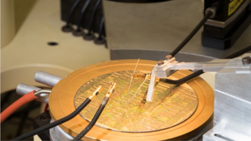
Wafer processing
Strong and thorough expertise for all technology steps:
- Photolithography,
- Etching,
- Thin film deposition...
More than 2000 m2 of clean rooms with state of the art equipment’s compatible with 2 inches to 100 mm for InP (Indium Phosphide), GaAs (Gallium Arsenide),
SiC (Silicon Carbide) based materials, including:
- high performance e-beam
- and stepper.