How to master III-V elements
|
![]() |
Material GrowthIII-V lab has developed epitaxial growth processes by Metal Organic Vapour Phase Epitaxy (MOVPE) and Molecular Beam Epitaxy (MBE) and Halide Vapour Phase Epitaxy (HVPE), on various substrates such as GaAs, InP and GaSb for both optoelectronic and microelectronic devices, as well as on SiC and Si for GaN microwave devices. An experienced team is available to provide device designers with the properly engineered arsenide, phosphide and antimonide heterostructures, mixing various types of abrupt or graded heterojunctions, incorporating quantum wells or quantum dots, or strained material layers. Besides in situ monitoring of grown layers, a full set of in house characterization tools are available including high precision X-ray double diffraction, room and low temperature photoluminescence, dopant and mobility profiling. More advanced characterization is subcontracted to local partners. |
![]() |
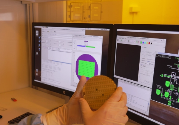
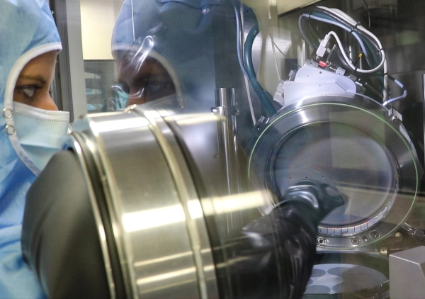
Wafer processingComplete processing lines are available for the production of III-V based optoelectronic and microelectronic devices and circuits, located in the 800 m² and 400 m² of processing clean rooms (class 10000 or better) in Marcoussis and Palaiseau respectively. Processing building blocks have been developed, qualified and tuned to cover the many requirements of the variety of devices and III-V material systems :
|
![]() |
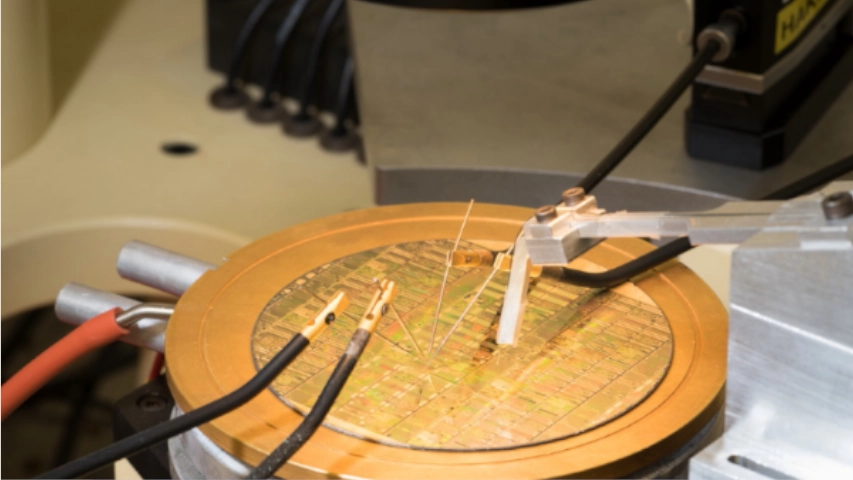
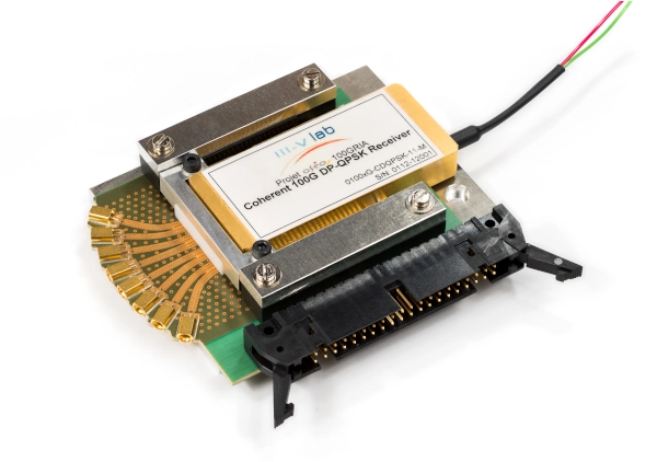
MeasurementIn order to assess device and circuit performances and to provide application teams with functional devices, packaging is a key technology for the III-V Lab. Many test set-ups have been developed at III-V Lab for the characterization of the different types of devices and circuits such as:
|
![]() |
Multi-Physics modellingWhile thermal and electronic modeling, device and circuit designs mostly rely on commercially available softwares, sometimes complemented by specific internal codes, a number of in-house softwares have been developed for guided-wave optoelectronic devices, anticipating the capabilities of commercial ones. |