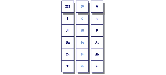
III-V columns in the Mendeleïev's periodic table
III-V on Silicon, Gallium nitride, Indium Phosphide, Gallium arsenide… how to combine semiconductor compounds
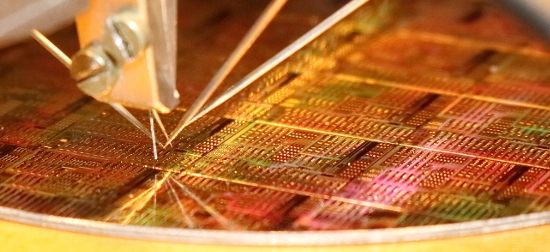
III-V lab has developed epitaxial growth processes by:
- Metal Organic Vapour Phase Epitaxy (MOVPE),
- Molecular Beam Epitaxy (MBE),
- Halide Vapour Phase Epitaxy (HVPE),
- Gas Source Molecular Beam Epitaxy (GSMBE),
on various substrates such as:
- Gallium Arsenide (GaAs), Indium Phosphide (InP) and Gallium Antimonide (GaSb) for both optoelectronic and microelectronic devices,
- Silicon Carbide (SiC) and Silicon (Si) for Gallium Nitride (GaN) microwave devices.
An efficient collaboration in Photonics, Optronics and Nanoelectronics
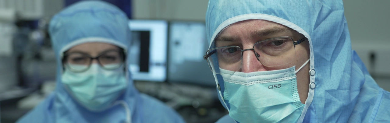
III-V Lab is a private Research & Development laboratory dedicated to III-V activities.
Its staff amounts to approximately 130 persons.
Both located at the heart of the Paris-Saclay Scientific campus, and at the heart of Minatec campus in Grenoble,
III-V Lab covers investigation from basic research to technology transfer for industrialization and concentrates in a single entity
the most advanced industrial research capabilities in the field of III-V semiconductors in Europe.
The collaboration is at the creation of III-V Lab, jointly established by Nokia, Thales and the CEA under the French
“Economic Interest Grouping” (GIE) status.