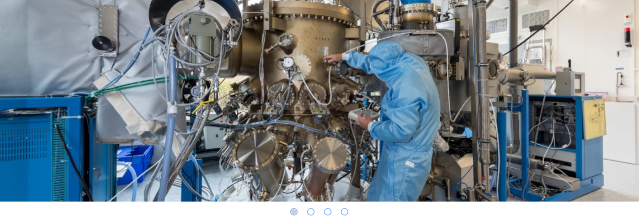
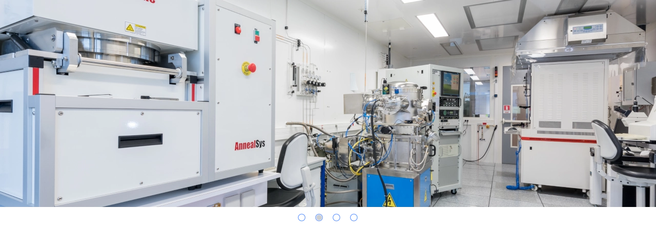
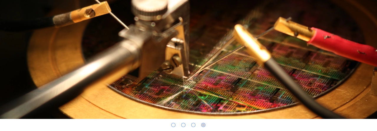
NEWS  PUBLICATIONS  PRESS RELEASE  PROJECTS  CONTACT US
NEWS: Installation and Start-up of a CCS 19x2'' Showerhead reactor
 Research & Development 
Laser Diodes & Optical Amplifiers
Photodiodes
Infra-Red Imagery Sensors
InP HBTs for Mixed Signals
GaN for Power & Microwave
 Products & Services 
Foundry Services
Datasheets
 Core Competencies 
III-V Epitaxy
III-V/Si Device Integration
Processing
Design & Characterization
Packaging
 About Us 
Mission
Facilities
Contact & Location

InP HBTs for mixed signals applications

A Double Heterojunction Bipolar Transistor process has been developed in the InP/InGaAs material system, and is used for the fabrication of very high frequency mixed signals ICs
The HBT structure comprises a strained graded gap InGaAs base and a step graded base-collector junction. With a triple mesa process and 2 µm wide emitter metal contact, HBTs exhibit max cut-off frequencies above 220 GHz for both Ft and Fmax, while retaining a breakdown voltage larger than 5 V. Circuits are designed based on such HBTs, together with thin film resistors and capacitors, and 3-layer metal interconnects.
Circuits with a transistors count of up to 100 have been fabricated, mainly intended for 43 Gbit/s optical fiber applications. Owing to the large intrinsic performances of the devices and to a specific design methodology and accurate modeling, circuits have been designed and fabricated offering state of the art results.

Microphotograph of a 0.7 µm emitter width InP/InGaAs HBT
Example of a 40 Gbit/s mixed signal IC. Besides HBTs, this circuit integrates resistors, capacitors, a 3-layer metal interconnects, and coplanar access lines.
Output eye diagram of a D-FF operating at 40 Gbit/s, exhibiting a record low value of 260 fs jitter.

 CERTIFICATE   LEGAL NOTICE  All rights reserved © Copyright 2007 G.I.E Alcatel Thales III-V Lab, France.